- 您现在的位置:买卖IC网 > Sheet目录1992 > CY28442ZXC-2 (Silicon Laboratories Inc)IC CLOCK ALVISO PENTM 56TSSOP
CY28442-2
....................... Document #: 38-07691 Rev. *B Page 9 of 19
The CY28442-2 requires a Parallel Resonance Crystal.
Substituting a series resonance crystal will cause the
CY28442-2 to operate at the wrong frequency and violate the
ppm specification. For most applications there is a 300-ppm
frequency shift between series and parallel crystals due to
incorrect loading.
Crystal Loading
Crystal loading plays a critical role in achieving low ppm perfor-
mance. To realize low ppm performance, the total capacitance
the crystal will see must be considered to calculate the appro-
priate capacitive loading (CL).
Figure 1 shows a typical crystal configuration using the two
trim capacitors. An important clarification for the following
discussion is that the trim capacitors are in series with the
crystal not parallel. It’s a common misconception that load
capacitors are in parallel with the crystal and should be
approximately equal to the load capacitance of the crystal.
This is not true.
Calculating Load Capacitors
In addition to the standard external trim capacitors, trace
capacitance and pin capacitance must also be considered to
correctly calculate crystal loading. As mentioned previously,
the capacitance on each side of the crystal is in series with the
crystal. This means the total capacitance on each side of the
crystal must be twice the specified crystal load capacitance
(CL). While the capacitance on each side of the crystal is in
series with the crystal, trim capacitors (Ce1,Ce2) should be
calculated to provide equal capacitive loading on both sides.
.
As mentioned previously, the capacitance on each side of the
crystal is in series with the crystal. This mean the total capac-
itance on each side of the crystal must be twice the specified
load capacitance (CL). While the capacitance on each side of
the crystal is in series with the crystal, trim capacitors
(Ce1,Ce2) should be calculated to provide equal capacitance
loading on both sides.
Use the following formulas to calculate the trim capacitor
values for Ce1 and Ce2.
CL....................................................Crystal load capacitance
CLe......................................... Actual loading seen by crystal
using standard value trim capacitors
Ce..................................................... External trim capacitors
Cs .............................................. Stray capacitance (terraced)
Ci ...........................................................Internal capacitance
(lead frame, bond wires etc.)
CLK_REQ[0:1]# Description
The CLKREQ#[A:B] signals are active LOW inputs used for
clean enabling and disabling selected SRC outputs. The
outputs controlled by CLKREQ#[A:B] are determined by the
settings in register byte 8. The CLKREQ# signal is a
de-bounced signal in that it’s state must remain unchanged
during two consecutive rising edges of SRCC to be recognized
as a valid assertion or deassertion. (The assertion and
deassertion of this signal is absolutely asynchronous).
Table 5. Crystal Recommendations
Frequency
(Fund)
Cut
Loading
Load Cap
Drive
(max.)
Shunt Cap
(max.)
Motional
(max.)
Tolerance
(max.)
Stability
(max.)
Aging
(max.)
14.31818 MHz
AT
Parallel
20 pF
0.1 mW
5 pF
0.016 pF
35 ppm
30 ppm
5 ppm
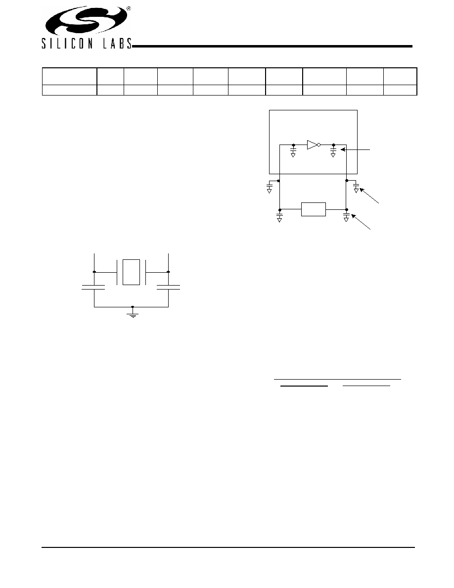
Figure 1. Crystal Capacitive Clarification
XTAL
Ce2
Ce1
Cs1
Cs2
X1
X2
Ci1
Ci2
Clock Chip
Trace
2.8pF
Trim
33pF
Pin
3 to 6p
Figure 2. Crystal Loading Example
Load Capacitance (each side)
Total Capacitance (as seen by the crystal)
Ce = 2 * CL – (Cs + Ci)
Ce1 + Cs1 + Ci1
1
+
Ce2 + Cs2 + Ci2
1
(
)
1
=
CLe
发布紧急采购,3分钟左右您将得到回复。
相关PDF资料
CY28445LFXC-5
IC CLOCK CALISTOGA CK410M 68QFN
CY28446LFXC
IC CLOCK CALISTOGA CK410M 64QFN
CY28447LFXC
IC CLOCK CALISTOGA CK410M 72QFN
CY28547LFXCT
IC CLOCK CK505/410M INTEL 72QFN
CY28548ZXC
IC CLK CK505 960M/965M 64TSSOP
CY28551LFXC-3T
IC CLOCK INTEL/AMD SIS VIA 56QFN
CY28551LFXC
IC CLOCK INTEL/AMD SIS VIA 64QFN
CY2SSTV855ZXI
IC CLOCK DIFFDRV PLL DDR 28TSSOP
相关代理商/技术参数
CY28442ZXC-2T
功能描述:时钟发生器及支持产品 Calistoga RoHS:否 制造商:Silicon Labs 类型:Clock Generators 最大输入频率:14.318 MHz 最大输出频率:166 MHz 输出端数量:16 占空比 - 最大:55 % 工作电源电压:3.3 V 工作电源电流:1 mA 最大工作温度:+ 85 C 安装风格:SMD/SMT 封装 / 箱体:QFN-56
CY28442ZXCT
功能描述:IC CLOCK GEN ALVISO 56-TSSOP RoHS:是 类别:集成电路 (IC) >> 时钟/计时 - 时钟发生器,PLL,频率合成器 系列:- 产品变化通告:Product Discontinuation 04/May/2011 标准包装:96 系列:- 类型:时钟倍频器,零延迟缓冲器 PLL:带旁路 输入:LVTTL 输出:LVTTL 电路数:1 比率 - 输入:输出:1:8 差分 - 输入:输出:无/无 频率 - 最大:133.3MHz 除法器/乘法器:是/无 电源电压:3 V ~ 3.6 V 工作温度:0°C ~ 70°C 安装类型:表面贴装 封装/外壳:16-TSSOP(0.173",4.40mm 宽) 供应商设备封装:16-TSSOP 包装:管件 其它名称:23S08-5HPGG
CY28443
制造商:CYPRESS 制造商全称:Cypress Semiconductor 功能描述:Clock Generator for Intel㈢ Calistoga Chipset
CY28443-2
制造商:CYPRESS 制造商全称:Cypress Semiconductor 功能描述:Clock Generator for Intel㈢ Calistoga Chipset
CY28443-3
制造商:SPECTRALINEAR 制造商全称:SPECTRALINEAR 功能描述:Clock Generator for Intel㈢ Calistoga Chipset
CY28443OXC
制造商:CYPRESS 制造商全称:Cypress Semiconductor 功能描述:Clock Generator for Intel㈢ Calistoga Chipset
CY28443OXC-2
制造商:CYPRESS 制造商全称:Cypress Semiconductor 功能描述:Clock Generator for Intel㈢ Calistoga Chipset
CY28443OXC-2T
制造商:CYPRESS 制造商全称:Cypress Semiconductor 功能描述:Clock Generator for Intel㈢ Calistoga Chipset